Patchy nanoparticles by atomic stencilling
Chemicals
All chemicals were used without further purification after purchase: gold(III) chloride trihydrate (≥99.9% trace metals basis, HAuCl4·3H2O, Sigma-Aldrich), sodium borohydride (99%, NaBH4, Sigma-Aldrich), sodium iodide (99.999%, NaI, Sigma-Aldrich), sodium bromide (≥99.99%, NaBr, Sigma-Aldrich), sodium chloride (99.3%, NaCl, Fisher Scientific), potassium iodide (≥99.5%, KI, Sigma-Aldrich), silver nitrate (≥99.0%, AgNO3, Sigma-Aldrich), sodium tetrachloropalladate(II) (approximately 36%, Na2PdCl4, Acros Organics), l-ascorbic acid (BioXtra, ≥99.0%, AA, Sigma-Aldrich), sodium hydroxide (99.99%, NaOH, Sigma-Aldrich), cetyltrimethylammonium chloride (>95%, CTAC, TCI, product number: H0082), benzyldimethylhexadecylammonium chloride (≥97.0%, BDAC, Sigma-Aldrich), cetylpyridinium chloride (>98.0%, CPC, TCI, product number: H0078), sodium citrate tribasic dihydrate (≥99.0, C6H5Na3O7, Sigma-Aldrich), PS154–b-PAA51 (Mn = 16,000 for the PS block and Mn = 3,700 for the PAA block, Mw/Mn = 1.04, Polymer Source Inc.), PS154–b-poly(acrylamide)49 (Mn = 16,000 for the PS block and Mn = 3,500 for the poly(acrylamide) block, Mw/Mn = 1.15, Polymer Source Inc.), PS154–b-poly(ethylene oxide)170 (Mn = 16,000 for the PS block and Mn = 7,500 for the poly(acrylamide) block, Mw/Mn = 1.09, Polymer Source Inc.), 2-NAT (99%, Sigma-Aldrich), biphenyl-4-thiol (97%, Sigma-Aldrich), DMF (anhydrous, 99.8%, Sigma-Aldrich) and hydrochloric acid (99.999% metals basis, HCl, Alfa Aesar). Nanopure deionized (DI) water (18.2 MΩ cm at 25 °C) purified by a Milli-Q Advantage A10 system was used. Note that the purity of cetyltrimethylammonium bromide (CTAB) is important for gold NP synthesis. We have used three types of CTAB: (1) Sigma-Aldrich, for molecular biology, ≥99%, product number: H6269; (2) Sigma-Aldrich, BioXtra, ≥99%, product number: H9151; and (3) Sigma-Aldrich, BioUltra, ≥99.0%, product number: 52365. For the data presented in this work, CTAB (1) and CTAB (2) were used for the experiments performed before February 2024. CTAB (3) has been used to reproduce the experiments afterwards.
Synthesis of core NPs
Gold octahedron, cuboctahedron, rhombic dodecahedron, cube and bipyramid NPs were synthesized following previously reported methods with slight modifications33,34 (Supplementary Note 1). Palladium cubes were synthesized following previous literature51 with modifications (Supplementary Note 2.8).
Synthesis of patchy NPs
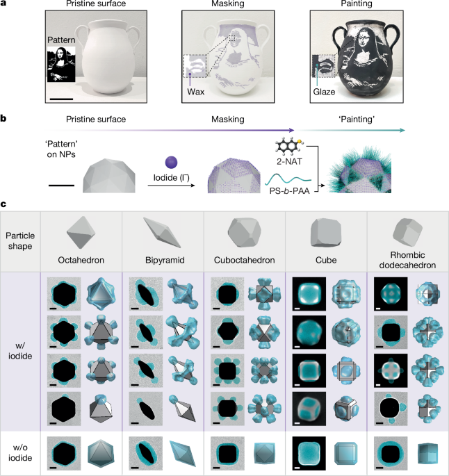
Patchy NPs were synthesized in two steps, which are iodide masking and ligand-mediated polymer grafting. Using the patchy octahedra in Fig. 3c as an example, for the iodide-masking step, we first degas DI water by purging with N2 for 1 h to minimize oxygen content. This degassed water is used throughout the masking step to minimize the oxidative etching of NPs. A gold octahedra solution was centrifuged at 2,400 × g for 15 min and the resulting pellet was diluted in 20 mM CTAC with degassed water to achieve a final NP concentration of 0.5 optical density (OD) at a maximum extinction wavelength λmax (Stock Solution I). Next, 5.75 µl of freshly prepared iodide solution (1 ml of 10 mM NaI, 500 µl of 200 mM NaOH and 8.5 ml degassed DI water) was added dropwise to 6.9 ml of Stock Solution I under mild vortex and incubated undisturbed for 30 min. After the incubation, 2.1 ml of 40 mM CTAB was added, followed by three rounds of centrifugation (3,400 × g, 5,300 × g and 2,200 × g for 15 min each). The supernatant was removed after each centrifugation and a 10-µl pellet was redispersed in 10 ml of 20 mM CTAB after the first round and 1 ml of DI water after the second round, respectively. The final pellet from the third centrifugation, after supernatant removal, was diluted with DI water to reach 5.0 OD at λmax with 0.07 mM CTAB (Stock Solution II). The final CTAB concentration can be varied depending on differently shaped NPs, as provided in Supplementary Note 2.
For ligand-mediated polymer grafting, still using the patchy octahedra in Fig. 3c as an example, we sequentially added 817 µl DMF, 5 µl of 2-NAT solution (2 mg ml−1 in DMF), 200 µl of Stock Solution II and 80 µl of PS-b-PAA (8 mg ml−1 in DMF) into an 8-ml vial under mild vortex. The vial was tightly capped with a Teflon-lined cap, sonicated for 5 s, Parafilm-sealed and heated at 110 °C in an oil bath for 2 h without disturbance. After cooling to room temperature in the oil bath, the reaction mixture was transferred to a 1.5-ml microcentrifuge tube and centrifuged three times at 3,400 × g, 1,300 × g and 1,000 × g (15 min each) to remove molecular residues. After each centrifugation, 1.49 ml of the supernatant was removed and a 10-µl pellet was redispersed in 1.49 ml of water. Following the final centrifugation, the 10-µl pellet was diluted with 90 µl of water for subsequent characterizations and self-assembly experiments. Detailed descriptions of the experimental procedure of the synthesis of other patchy NPs are provided in Supplementary Note 2 and Supplementary Tables 2–8.
Similar procedures with modifications can be extended to palladium nanocubes (Supplementary Note 2.8), other thiols and block copolymers (Supplementary Notes 2.1 and 2.5) and scale-up synthesis (Supplementary Note 2.9).
Large-scale self-assembly of patchy NPs
For self-assembly experiments, a patchy NP solution in a 1.5-ml microcentrifuge tube was left undisturbed overnight, allowing the particles to sediment and concentrate (≥30.0 OD at λmax).
Coffee ring effect-driven assembly on a silicon wafer
A silicon wafer (3 × 3 mm2, Ted Pella) was cleaned with water, acetone and isopropanol through sonication for 5 min each, followed by 60 s of O2 plasma treatment using a Harrick Plasma PDC-32 (maximum RF power of 18 W) to make the surface hydrophilic. Meanwhile, a 4 × 4-inch2 piece of Parafilm was placed on a TechniCloth (TX609, Texwipe) with a water-filled Petri dish cover (60 × 15 mm2, Falcon) on top. 3.5 µl of a concentrated patchy NP solution was drop-casted onto the wafer on the Parafilm. Immediately after drop-casting, both the silicon wafer and Petri dish were covered by a large Petri dish (100 × 15 mm2, VWR) and gently pressed down to seal against the Parafilm, maintaining a humid environment (humidity: 75–80%). A typical drying process takes 16–24 h at room temperature (Supplementary Fig. 38a).
Capillary force-driven assembly in a glass capillary tube
A 10-µl glass capillary tube (inner diameter: 0.5573 mm, Drummond Scientific Company) was filled with 2 M NaOH, incubated for 20 min, rinsed with water and dried to make the inner wall hydrophilic before use. 5 µl of concentrated patchy NP solution was then drawn into the capillary tube, keeping the NP solution several centimetres away from both tube ends. The capillary tube was suspended inside a loosely capped 15-ml centrifuge tube, which was then placed in a desiccator until the solution had fully dried, forming a visible gold ring around the interior. See the experimental set-up in Supplementary Fig. 38b.
Electron microscopy characterizations
TEM, SEM and STEM characterizations
TEM images were acquired with a JEOL 2100 LaB6 transmission electron microscope operated at 200 kV. SEM images were captured using an FEI Helios NanoLab 600i operated at 2 kV with a beam current of 0.17 nA and a working distance of 4.0 mm. HAADF-scanning transmission electron microscopy (STEM) imaging was conducted on a probe aberration-corrected Thermo Fisher Scientific Themis Z scanning transmission electron microscope operated at 300 kV. STEM-EDX mapping was acquired with a Thermo Fisher Scientific ‘Kraken’ Spectra 300 operated at 60 kV equipped with Dual-X EDX detectors with a collection angle of 1.76 sr.
Sample preparation for HAADF-STEM characterization
For NP facet imaging and analysis, solutions of pristine NPs were drop-casted on TEM grids, with CTAB concentration reduced through three rounds of centrifugation. Approximately 50–200 µl of the pristine NP solutions in 40 mM CTAB was used per sample. Each sample was first diluted with 1 ml of water in 1.5-ml microcentrifuge tubes, followed by removing 990 µl of supernatant after each of the first two centrifugations. After each centrifugation, a 10-µl pellet was redispersed in 990 µl of water. Following the third centrifugation, a 1.5-µl pellet was drop-casted onto a carbon-coated copper TEM grid (Electron Microscopy Sciences, CF400-Cu) and dried completely. Before imaging, samples were plasma-cleaned for 2 min at 15 W under a 12-sccm flow of Ar + O2 to remove residual CTAB molecules covering NPs using a PIE Scientific Tergeo-EM plasma cleaner.
HAADF-STEM imaging
HAADF images were acquired with a beam current of approximately 20 pA and semi-convergence angle of 18 mrad. The camera length was 115 mm and the collection angles of the HAADF detector were 62–200 mrad for image acquisition. To minimize image distortion from sample drift, several sequential frames (10–50 frames) with short dwell time (100–500 ns) were acquired, which were used to render drift-corrected frames to enhance the contrast.
TEM tomography
TEM images for tomography reconstruction were collected by titling the samples from 0° to −60° and then from 0° to +60° in 2° intervals, capturing 61 images per sample. To minimize beam damage, a low electron dose rate of 6–8 e− Å−2 s−1 was used. To improve the polymer patch contrast, a defocus of −2,048 nm was used. Image alignment and contrast-transfer function correction were performed using IMOD64 4.9.3 software52. Tomograms were generated using OpenMBIR with diffuseness of 0.3 and smoothness of 0.2 as reconstruction parameters, which uses a model-based iterative algorithm of tomogram reconstruction53. 3D models of the tomograms were visualized using Amira 6.4 from Thermo Fisher Scientific. The tomograms were denoised using three filters: median (3 × 3 × 3 voxel neighbourhood, iterations 26), Gaussian filter (kernel size 9, 3 × 3 × 3 standard deviation) and edge-preserving smoothing (time 25, step 5, contrast 3.5 and sigma 3). Polymer patches and gold NPs were segmented by greyscale intensity thresholding and refined manually in Amira 6.4 software.
STEM-EDX characterization
Samples for the STEM-EDX analysis were prepared by drop-casting Stock Solution II on carbon-coated copper TEM grids (Electron Microscopy Sciences, CF400-Cu). The octahedra and cuboctahedra were iodide-masked. To minimize carbon contamination, the TEM grids were baked overnight at 130 °C in high vacuum to remove excess CTAB. STEM-EDX maps were acquired with a 120-pA probe current, a 30-mrad semi-convergence angle and continuous raster-scanning with drift correction, using a 2-µs dwell time over approximately 4 h. For iodide-masked cuboctahedra, the NPs were predominantly oriented on the carbon support along the [001] direction. Therefore, the stage was tilted 45° to the [110] zone axis, aligning both the {111} and {100} facets ‘edge-on’. Elemental mapping was achieved by fitting and quantifying the peak intensities above the background using the Cliff–Lorimer method54. Two high-quality EDX maps of seven cuboctahedra were selected and a total of 1,692 line profiles were obtained (Supplementary Fig. 25). Similarly, iodide-masked octahedra were oriented on the carbon support along the [110] direction and their ‘edge-on’ {111} facets were used for iodide concentration analysis (Extended Data Fig. 2).
TEM image analysis
Patch local thickness t
loc
The tloc of patches was determined as the diameter of the largest circle that can fit within the patch and includes the target pixel. Patch contours were manually outlined in ImageJ to define the patch regions. The tloc map was then obtained using the built-in ‘Local Thickness’ function in ImageJ, as also detailed in our previous work24.
Maximum patch thickness t
m and patch coverage fraction f
cov
The values of tm and fcov were measured using a neural-network-based method on TEM images55. The neural network-based TEM image segmentation is detailed in Supplementary Note 3 and Supplementary Figs. 32 and 33. After training the neural network with manually labelled TEM images of diverse patchy NP shapes, a shape fingerprint t was extracted from the patch contours. First, the centroid of the gold NP was identified and rays extending from θ = −180° to θ = 179° at 1° intervals were drawn from the centroid. The distance that each ray travels within the patch region was recorded as a function of θ. tm is determined by the maximum value of t and fcov is identified as the range of θ in which t is non-zero. See detailed description in Supplementary Note 3 and Supplementary Figs. 34–36.
Other characterizations
UV–Vis measurements
Ultraviolet–visible (UV–Vis) spectra were measured using a Scinco S-4100 PDA spectrophotometer with a quartz cuvette (path length = 1 cm, VWR).
XPS characterization
XPS analysis was performed using a Kratos Axis Ultra equipped with a monochromatic Al Kα radiation X-ray source and an energy resolution of 0.4 eV. Before characterization, 10 µl of each Stock Solution II, prepared with various iodide concentrations, was drop-casted on a silicon wafer cleaned with water, acetone and isopropanol and then fully dried. The silicon wafers were fixed to the sample bar and transported to the instrument in an airtight container under an Ar atmosphere for XPS signal acquisition. Data processing and peak fitting were conducted using the CasaXPS software. Atomic concentrations within samples were calculated by integrating the fitted XPS spectra for all analysed regions and adjusting for atomic relative sensitivity factors. See detailed sample conditions in Supplementary Table 9.
Raman characterization
Raman characterization was performed using a Horiba XploRA-nano TERS/TEPL with a 100× objective lens. The Raman samples were prepared following two steps, without polymer grafting (Supplementary Table 10). First, gold octahedra were iodide-masked in varying [I−] and then concentrated to reach 20.0 OD at λmax in 0.07 mM CTAB, following the iodide-masking procedure described above. Next, 40 µl of 2-NAT (0.2 mg ml−1 in DMF) and 200 µl of the iodide-masked octahedra were sequentially added into 860 µl of DMF in a vial with mild vortex. The remaining reaction condition and washing steps follow the standard iodide masking procedure, except for centrifugation, which was performed three times at 2,900 × g for 15 min and 2,400 × g for 7 min twice. After the first two centrifugations, the pellet was resuspended in 1 ml of DMF. After the final centrifugation, the sediment was redispersed in 20 µl of DMF and the NP concentration was adjusted to 13.0 OD at λmax by adding water. A 5-µl aliquot of this NP solution was drop-casted onto a clean glass slide. The glass slide was used after washing with isopropyl alcohol and water and then fully dried. Raman measurements were performed with a 638-nm excitation wavelength, 1-mW laser power and three scans for average (90 s exposure time each).
X-ray tomography of large-scale self-assembly
The X-ray tomography sample was prepared through a focused-ion beam milling using the FEI Helios NanoLab 600i. Before milling, platinum was deposited on the self-assembled patchy rhombic dodecahedra on a silicon wafer, with a deposition diameter of 3 µm and a thickness of 300 nm. Subsequently, the assembly was milled into a cylinder with a diameter of 2.5 µm. The shaped cylinder was lifted with an OmniProbe and mounted onto a tungsten needle tip (Supplementary Fig. 50).
X-ray tomography data were acquired at the hard X-ray nanoprobe beamline of National Synchrotron Light Source II at Brookhaven National Laboratory. A monochromatic beam at 12 keV was selected and then focused by a set of crossed multilayer Laue lenses to produce a nanobeam56 with a size of approximately 13 nm. 2D fly-scans were performed in a grid pattern with at least 150 × 150 pixels, 50-ms dwell time and 10-nm step size at every 2° to collect 91 projections covering 180°. Far-field diffraction patterns were analysed with a ptychographic reconstruction algorithm to retrieve both the complex-valued probe and the object functions. The acquired fluorescence spectra were fitted using the software package PyXRF. Individual 2D frames were coarsely aligned using ImageJ 1.5, MultiStackReg plugin, whereas fine alignments were adjusted with a cross-correlation function in Tomviz 1.9, followed by 3D reconstruction. The data were further processed by Fourier filtering using the sharp lattice peaks in the reciprocal space image of the superlattice to remove noise and sharpen the particle positions for subsequent segmentation, using Dragonfly 2020.2 software57.
DFT calculations of gold surfaces with iodide and 2-NAT
All DFT calculations were performed using the Vienna Ab initio Simulation Package58,59,60 with projector augmented waves61. The generalized gradient approximation by Perdew, Burke and Ernzerhof was used for the exchange-correlation functional62. We chose an energy cut-off of 450 eV as an optimal value for our plane-wave basis set. For the sampling of the first Brillouin zone, Monkhorst–Pack grids were used63. We also included the DFT-D3 method of Grimme et al. with the Becke–Johnson damping to describe long-range van der Waals interactions64. See details in Supplementary Note 4.
Computation and theory modelling of patchy NPs and their assemblies
Patchy NP grafting simulation
A library of individual patchy NPs was simulated using MD using the HOOMD-blue simulation engine65. First, a single anisotropic particle was placed at the centre of the simulation box. Polymer chains with one grafting end were then randomly distributed on the surface of the central anisotropic particle and allowed to freely move on the surface to find their equilibrium positions. The location of iodide-masked regions predicted from our iodide adsorption theory (see details in Supplementary Note 5) were modelled as spherical beads that are strongly repulsive to the polymer chains. All chain–chain interactions exhibit Lennard–Jones attraction with each other to capture the PS–PS aggregation in experimental conditions. All other interactions were purely repulsive and modelled using the Weeks–Chandler–Andersen repulsive potential. For detailed description, see Supplementary Note 8.
Theoretical prediction of patches
Polymer patch patterns and sizes were theoretically predicted using MC grafting simulation involving two steps: (1) determining the surface distribution of iodide-masked region and (2) placing polymer chains onto the unmasked (‘free’) surface sites, while accounting for chain–chain interactions. We began by constructing a grid of points on the core NP surface, defining potential sites for iodide or polymer attachment. Using the Metropolis algorithm with surface energies computed from DFT, iodide-masked points were placed on the various surface sites (Supplementary Note 5). Placing iodide-masked points on the particle surface uses the Metropolis algorithm, guided by surface energies computed from DFT. Iodide-masked points cannot accommodate polymer grafting, leaving the remaining open locations as the only ‘free’ sites for polymer grafting. After an occupancy matrix logs iodide-masked positions, the first polymer chain grafts on the surface based on its Boltzmann-weighted free energy as a function of surface locations. The matrix updates with this chain attachment and ‘free’ surface sites within a correlation length ξ of any polymer-occupied sites gain a favourable chain–chain interaction, governed by the Flory–Huggins parameter χ (Supplementary Note 6). This entire process repeats for each polymer chain until the target grafting density is achieved. See Supplementary Note 7 for details.
Simulation of patchy NP self-assembly
MC simulations were performed to obtain the self-assemblies of patchy NPs, using the HOOMD-blue simulation engine65. We first defined a patchy particle whose patch locations and sizes are commensurate with those measured from the above MD simulation and validated with theory and experiments. Patches were modelled to exhibit hard sphere interactions with each other to capture the strong PAA–PAA electrostatic repulsions between the outer surface of the patches (Supplementary Fig. 49). The core NP interactions were modelled using a Kern–Frenkel attraction between the various surface sites that were not covered by polymeric patches. See Supplementary Note 9 for details.
First Appeared on
Source link

